Fabless Platform for Wafer Process Integration
TOYOKOU CHEMI (Japan), an affiliated company of AST, is positioned as a fabless, proposal-driven platform. It does not operate its own wafer fabrication facilities; instead, it integrates foundry resources across Japan and other parts of Asia to provide process solution design and manufacturing resource matching. The platform engages from the early stages of projects, supporting requirement analysis and process flow planning, and advances execution in coordination with partner fabs.
Leveraging Japan’s strengths in advanced materials and precision processing, together with manufacturing capabilities across Asia, TOYOKOU focuses on H-cut and thinning-bonding process routes. It supports heterogeneous integration of semiconductor and related materials, covering 4-, 6-, 8-, and 12-inch wafer projects. Process flows and foundry resources are selected and coordinated based on specific project requirements.
In terms of services, the platform provides foundry coordination for heterogeneous bonding and full-wafer processing, while also supporting upfront technical evaluation and solution development. Supported material systems include SOI, POI, SiC (single-crystal/polycrystalline structures), TFLN/TFLT, SiCOI, and other customized substrates, with applications in photonics, power devices, MEMS, and advanced packaging.
Process & Technology Coordination
Based on the established capabilities of partner fabs, TOYOKOU coordinates the implementation of process routes including room-temperature (RT) bonding, thermo-compression bonding, temporary bonding, and surface-activated bonding. Specific approaches are defined according to project requirements.
Capacity & Delivery
Relying on partner production lines, the platform supports prototyping and mid-volume manufacturing. The current delivery capability corresponds to approximately 10,000 wafers per year, subject to project requirements and resource allocation.
Team & Quality Systems
The platform focuses on project management and technical coordination. Manufacturing and quality control are executed by partner fabs in accordance with their respective quality management systems, including ISO 9001, IATF 16949, ISO 14001, and ISO 45001.
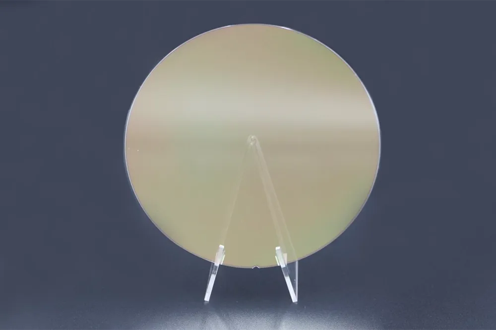
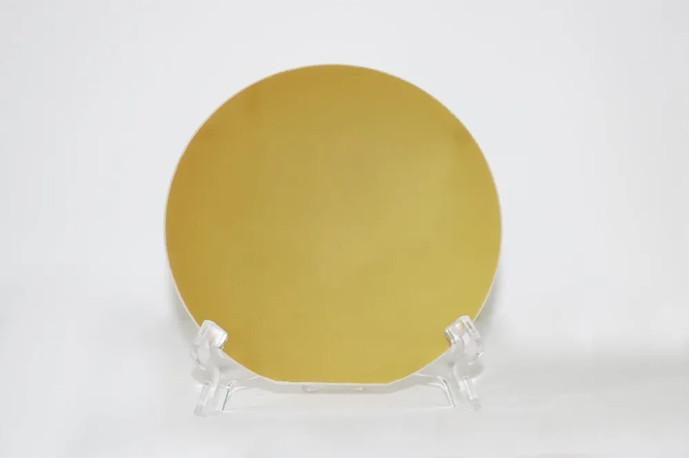
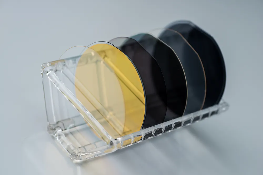
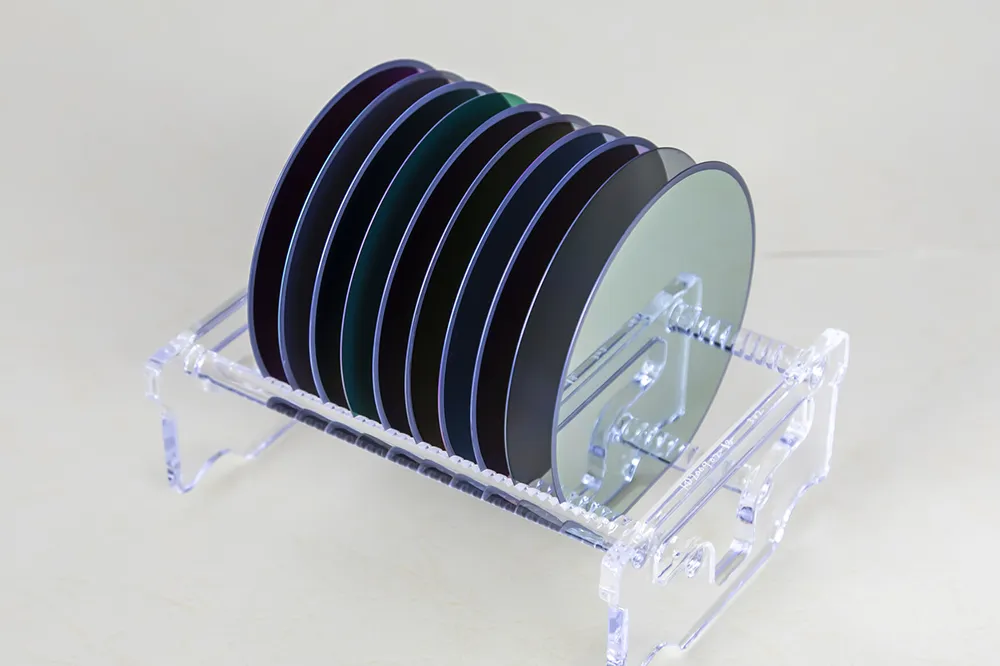
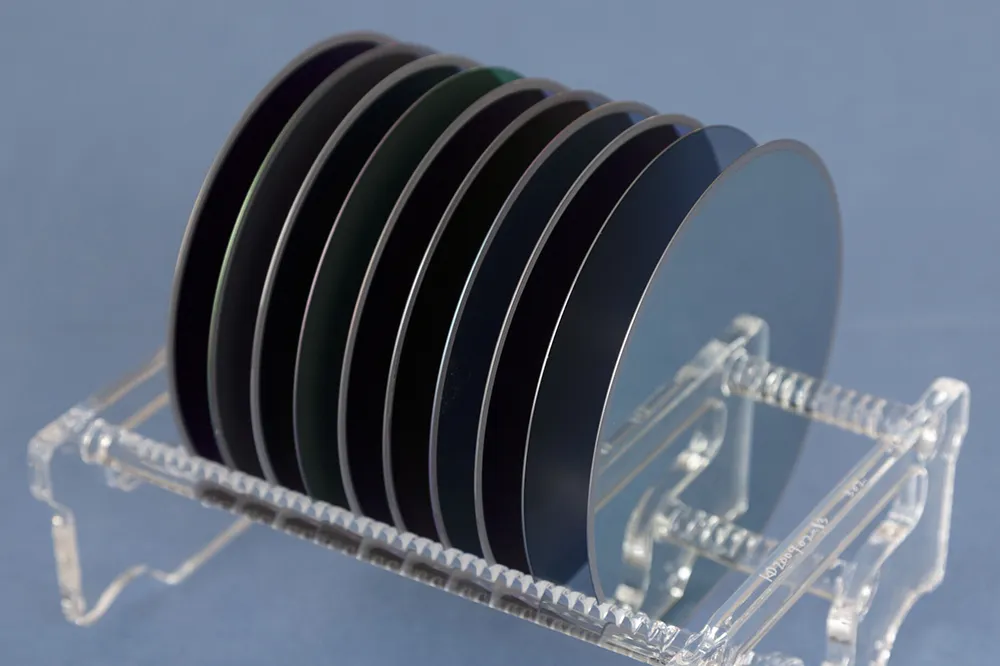
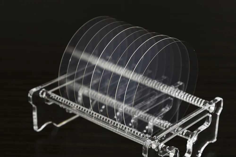
Composite Wafer
N-type SiC Composite Wafer

| Item | Specification | Item | Specification |
|---|---|---|---|
| Diameter | 150 ± 0.2 mm | Front (Si-face) roughness | Ra ≤ 0.2 nm (5 μm × 5 μm) |
| SiC Type | 4H | Edge Chip, Scratch, Crack (visual inspection) | None |
| SiC Resistivity | 0.015–0.025 Ω·cm | TTV | ≤3 μm |
| Transfer layer Thickness | ≥0.4 μm | Warp | ≤35 μm |
| Void | ≤5 ea/wafer (2 mm > D > 0.5 mm) | Thickness | 350 μm ± 25 μm |
Semi-insulating SiC Composite Wafer

| Item | Specification | Item | Specification |
|---|---|---|---|
| Diameter | 150 ± 0.2 mm | Front (Si-face) roughness | Ra ≤ 0.2 nm (5 μm × 5 μm) |
| SiC Type | 4H | Edge Chip, Scratch, Crack (visual inspection) | None |
| SiC Resistivity | 0.015–0.025 Ω·cm | TTV | ≤3 μm |
| Transfer layer Thickness | ≥0.4 μm | Warp | ≤35 μm |
| Void | ≤5 ea/wafer (2 mm > D > 0.5 mm) | Thickness | 500 ± 25 μm |
N-type SiC on Si Composite Wafer

| Item | Specification | Item | Specification |
|---|---|---|---|
| Diameter | 150 ± 0.2 mm | Si Orientation | <111>/<100>/<110> |
| SiC Type | 4H | Si Type | P/N |
| SiC Resistivity | 0.015–0.025 Ω·cm | Flat length | 47.5 ± 1.5 mm |
| Transfer SiC layer Thickness | ≥0.1 μm | Edge Chip, Scratch, Crack (visual inspection) | None |
| Void | ≤5 ea/wafer (2 mm < D < 0.5 mm) | TTV | ≤5 μm |
| Front roughness | Ra ≤ 0.2 nm (5 μm × 5 μm) | Thickness | 500/625/675 ± 25 μm |
Semi-insulating SiC on Si Composite Wafer

| Item | Specification | Item | Specification |
|---|---|---|---|
| Diameter | 150 ± 0.2 mm | Si Orientation | <111>/<100>/<110> |
| SiC Type | 4H | Si Type | P/N |
| SiC Resistivity | ≥1E8 Ω·cm | Flat/Notch | Flat/Notch |
| Transfer SiC layer Thickness | ≥0.1 μm | Edge Chip, Scratch, Crack (visual inspection) | None |
| Void | ≤5 ea/wafer (2 mm > D > 0.5 mm) | TTV | ≤5 μm |
| Front roughness | Ra ≤ 0.2 nm (5 μm × 5 μm) | Thickness | 500/625/675 ± 25 μm |
Si on SiC Composite Wafer

| Item | Specification | Item | Specification |
|---|---|---|---|
| Diameter | 150 ± 0.2 mm | SiC Type | 4H |
| Si Orientation | <111>/<100>/<110> | SiC Resistivity | 0.015–0.025/≥1E8 Ω·cm |
| Si Type | P/N | Flat/Notch | Flat/Notch |
| Transfer Si layer Thickness | ≥0.1 μm | Edge Chip, Scratch, Crack (visual inspection) | None |
| Void | ≤5 ea / wafer (2 mm > D > 0.5 mm) | TTV | ≤5 μm |
| Front roughness | Ra ≤ 0.2 nm (5 μm × 5 μm) | Thickness | 350/500 ± 25 μm |
Si on AlN Composite Wafer

| Item | Specification | Item | Specification |
|---|---|---|---|
| Diameter | 150 ± 0.2 mm | AlN Resistivity | ≥1E8 Ω·cm |
| Si Orientation | <111>/<100>/<110> | AlN Thermal conductivity | ≥180 W/m·K |
| Si Type | P/N | Flat length | 47.5 ± 1.5 mm |
| Transfer Si layer Thickness | ≥0.1 μm | TTV | ≤5 μm |
| Edge Chip, Scratch, Crack (visual inspection) | None | Thickness | 625 ± 25 μm |
| Front roughness | Ra ≤ 0.2 nm (5 μm × 5 μm) |
SOI Wafer
| Size | inch | 4 | 5 | 6 | 8 | 12 |
|---|---|---|---|---|---|---|
| Active Layer | Unit | Specification | ||||
| Manufacturing Method | - | CZ/FZ | ||||
| Type / Conductivity | - | P/N/Non-doped | ||||
| Crystal Orientation | - | <100>/<111>/<110> | ||||
| Dopant | - | B, P, As, Sb | ||||
| Thickness | μm | ≧1.0 | ||||
| *Resistivity | Ω·cm | 0.001–10000 | ||||
| *Embedded Oxide Film | μm | 0.05–10 | ||||
| Support Substrate | Specification | |||||
| Manufacturing Method | - | CZ/FZ | ||||
| Type / Conductivity | - | P/N/Non-doped | ||||
| Crystal Orientation | - | <100>/<111>/<110> | ||||
| Dopant | - | B, P, As, Sb | ||||
| *Thickness | μm | JEITA・SEMI Standard/200-1500 | ||||
| *Resistivity | Ω·cm | 0.001–10000 | ||||
| Remarks | *Please inquire separately for detailed specifications. | |||||
300-900nm LiNbO3 Single Crystal Thin Film (LNOI)

● Lithium Niobate Thin Film
● SiO2
● Si, LN, Quartz, Fused Silica, etc.
| Top Functional Layer | Diameter | 3, 4, (6) inches | Orientation | X, Z, Y, etc. |
|---|---|---|---|---|
| Material | LiNbO3 | Thickness | 300-900 nm | |
| Doping (Optional) | MgO | |||
| Separation Layer | Material | SiO2 | Thickness | 1000-4000 nm |
| Substrate | Material | Si, LN, Crystal, Fused Quartz, etc. | ||
| Thickness | 400-500 μm | |||
| Optional Electrode Layer | Material | Pt, Au, Cr | Thickness | 100-400 nm |
| Structure | Above or below the SiO2 separation layer | |||
300-900nm LiTaO3 Single Crystal Thin Film (LTOI)
● Lithium Tantalate Thin Film
● SiO2
● Silicon
| Top Functional Layer | Diameter | 3, 4, 6 inches | Orientation | Y-42, Y-46.3, Z, etc. |
|---|---|---|---|---|
| Material | LiTaO3 | Thickness | 300-900 nm | |
| Separation Layer | Material | SiO2 | Thickness | 300-4000 nm |
| Substrate | Material | Si | ||
| Thickness | 400-500 μm | |||
5-50μm LT & LN thin film on Si substrate

● Lithium Tantalate Thin Film
● Silicon
● Lithium Niobate Thin Film
● SiO2
● Silicon, Quartz, etc.
| Top Functional Layer | Diameter | 3, 4, 6 inches | Orientation | Y-42, Y-46.3, Z, etc. |
|---|---|---|---|---|
| Material | LiTaO3 | Thickness | 300-900 nm | |
| Separation Layer | Material | SiO2 | Thickness | 300-4000 nm |
| Substrate | Material | Si | ||
| Thickness | 400-500 μm | |||
20-60μm ultra-thin, super flat wafer

● Lithium Tantalate Thin Film Or Lithium Niobate Thin Film
| Diameter | 3, 4 inches | Orientation | X, Y, Z, etc. |
| Thickness | 10-60 μm | Material | LN, LT, Si, etc. |
| Surface | Double-sided or single-sided polishing | ||
Custom-made LN & LT thin film
| Top Layer/Details | Substrate Details | Top Layer Thin Film Details | ||||||
| Multilayer Structure | Electrode & Waveguide Pattern | Different Materials (SiO2/Si, Si, Sapphire, Quartz, etc.) | PPLN | Special Sizes | Electrodes (Au, Pt, Cr, Al, etc.) | Orientation (same as bulk wafer) | Doping (MgO, Fe, Er, Tm, etc.) | |
| 100-1000 nm LiNbO3 | √ | √ | √ | √ | √ | √ | √ | √ |
| 100-1500 nm LiTaO3 | √ | √ | √ | √ | √ | √ | √ | |
| 5-50 μm LiNbO3 | √ | √ | √ | √ | ||||
| 5-50 μm LiTaO3 | √ | √ | √ | √ | ||||